
January 30, 1997
The PMT signal is AC coupled through a 2.2 uF capacitor in the output of the B.U. Fanout. This eliminates D.C. offset from the high speed buffer amplifiers. For most fast pulses, the effect is simply to force the baseline to 0V with respect to system ground. However, for large enough pulses (or high enough rates- not an issue for us), the capacitor charges up, and then discharges through 50 Ohms, with a time constant of approximately 100 usec. This distorts the shape of the output pulse, as seen in figure 2. The first deleterious effect is that for large negative pulses, a positive overshoot is induced which can keep the positive threshold of the +-2.5 mV WFD threshold on. This reduces the level of zero-suppression and causes the initial waveform data (the data of interest) to fall outside our limited storage window. This effect has been seen for some time, mostly in large showering events. But it was recently recognized by Doug Michael and Sophia Kyriazopolou, from bright LED calibration data, that we also would lose some range of monopole sensitivity.
Figure 1. A copy of each input signal is passed to a circuit like this one. The diode is to help reduce crosstalk for large negative pulses. The proposed fix in this memo is to reduce the net capacitance of C115 and C116.
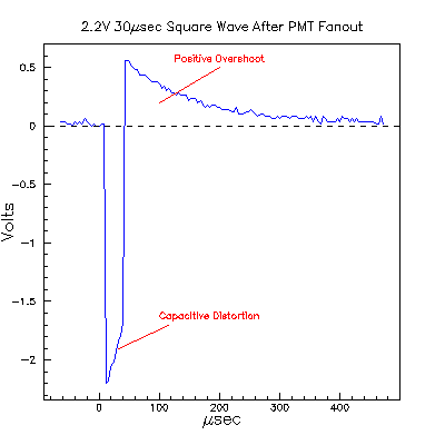
Figure 2. The output of the fanout in response to a -2.2V by 30 microsecond square wave input. The positive overshoot coming out of the PMT fanout is clearly visible. The time constant for its decay is approximately 100usec, long enough to fill our current WFD buffer maximum of 40 kilobytes. 40 kilobytes corresponds to 20 kilosamples, or equivalently 100 microseconds of time.
We considered disconnecting the positive discriminator from the WFD daughter card, but that lead Iaonnis and Erik Katsavounidis to recognize a second, related problem. If one takes the output from the fanout (figure 2) and passes it through the discriminator preamplifier, a second stage of capacitive coupling can cause a negative undershoot, shown in Figure 3. Even if the positive threshold is eliminated, the negative undershoot can again trigger the -2.5 mV threshold and force excess data to be recorded that causes the WFD to lose the initial pulse.
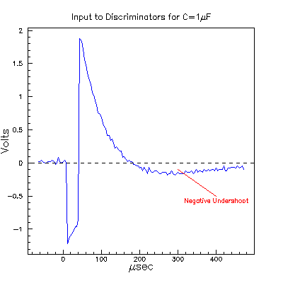
Figure 3. The input to the discriminator for the signal shown in figure 2. The positive overshoot is distorted before input to the discriminators so that it falls below ground and discharges with a very long time constant of about 400 microseconds.
These curves were made using square wave signals generated by an Hewlett-Packard pulser with programmable amplitudes between -0.090V and -7.20V, and pulse widths between 300ns and 30usec. The frequency of the pulses was set to 1Hz to reduce the level of noise on the baseline and to eliminate the chance of one pulse affecting subsequent pulses. The rise and fall times of the pulses were set to 100ns. Faster risetimes were possible, but contributed additional overshoot from the pulser itself.
The pulses were fed through a standard MACRO PMT fanout to a WFD daughter card mounted on a custom built test station. The daughter card test station provides all of the necessary operating voltages to one or two daughter cards, and allows a single threshold to be programmed on all inputs. This threshold was set to 6mV as measured by a Fluke DVM at J3 pin 3 of the daughter card.
Bill Earle, project engineer for the WFD electronics, suggested that we decrease the capacitance in the RC filter at the discriminator input. The capacitor's only function is to eliminate DC offset from the 3:1 amplifier that would affect our ability to discriminate on single photoelectron signals. Decreasing its value would not impede this function. (ETK and IK also discussed solutions along these lines after the Frascati meeting, before the negative undershoot problem had been identified).
Changing this capacitor has non-intuitive implications. Our goal is to eliminate the long pulses that saturate the WFD without eliminating real monopole data. Ideally, one would work with undistorted pulses at all times, and the discriminator pulses would ideally match when the input pulse is under or over threshold. By reducing the capacitance, we cause deliberate sharp positive and negative overshoots that control the discriminator data. Reducing the time constant of the RC filter too low will also limit the data from long monopole pulses. The time constant sets an upper limit on the maximum digitizable signal width. Figure 4 illustrates a case where a large, long pulse has data lost after recording the beginning of the pulse. While losing any data is not ideal, it is important to realize that with this scheme we would still record the beginning of a wide monopole pulse and catch the exit time from the trailing edge, providing adequate information for making a beta calculation.

Figure 4. The same pulse shown above is passed through a modified input with C115 removed and C116 changed to .01uF, resulting in a total capacitance a factor of hundred below its current value of 1uF and a time constant of about 1.2usec. For wide pulses like this 30usec pulse, the signal will not trigger either the positive or negative discriminators after the signal has decayed below threshold, but that the trailing edge of the pulse will trigger. For a monopole of this width we would expect single photoelectrons and not a -2V Pulse. Unphysical pulse parameters were chosen to amplify the data loss for clarity.
Another important factor in our favor is that real monopole pulses will have more high frequency structure than our square wave test pulses due to PMT fluctuations. To some degree, the RC filter will retrigger on the higher-frequency PMT fluctuations in real monopole pulses, reducing the time of lost data. However, the voltage-limiting diode at D110 will suppress this for pulse heights below approximately -380mV. We hope to quantify this effect through PSPICE simulations in the near future.
CMO modified the value of the capacitance at three of the four inputs of one daughter card. Input one was unmodifed, C=.1uF was installed on input two, C=.01uF on input three, and C=.05uF was installed on input four. No other modifications were made. The positive discriminator was left intact on all four inputs. Following similar tests made at LNGS by Iaonnis and Erik, he measured the critical pulse height for several different pulse widths, finding the maximum voltage at each width where the total discriminated width reached 100usec. This is the point where the WFD will start to lose the original signal. The data for unmodified channels is shown in Table 1, and for modified channels in Table 2.
    Pulse Width (usec)      Critical Pulse Height (V)
          .3                        7.0
         1.0                        3.0
         2.0                        0.29
         3.0                        0.19
         4.0                        0.16
         5.0                        0.13
         6.0                        0.09
         8.0                       <0.09
        10.0                       <0.09
        15.0                       <0.09
        20.0                       <0.09
        25.0                       <0.09
        30.0                       <0.09
Table 1. For each pulse width, the critical pulse height in Volts is
found where capacitive effects cause a total of 100usec of
discriminator time. The critical values for widths from 8 to 30 usec
was not determined because the input pulse size could not easily be
set to less that 90 mV.
                            Critical Pulse Height (V)
    Pulse Width (usec)      C=.1uF  C=.05uF  C=.01uF
          .3                >7.2    >7.2     >7.2
         1.0                 3.4     6.8     >7.2
         2.0                 2.3     4.3     >7.2
         3.0                 1.4     1.3     >7.2
         4.0                 1.3     0.91    >7.2
         5.0                 0.95    0.90    >7.2
         6.0                 0.76    0.88     7.1
         8.0                 0.57    0.82     4.4
        10.0                 0.48    0.59     3.3
        15.0                 0.36    0.48     1.5
        20.0                 0.34    0.38     1.3
        25.0                 0.24    0.29     1.2
        30.0                 0.17    0.26     1.0
Table 2. For each pulse width, the critical pulse height in
Volts is found where capacitive effects cause a total of 100usec of
discriminator time. Critical values in excess of 7.2V amplitude were
not determined because the input pulse size could not easily be set to
greater than 7.2V.
By comparing the data to the signal expected for monopoles and dyons we can gauge the best choice for C. In Figure 5, we assume that a typical muon is a 2V, 75ns wide triangular signal and that the charge derived from the integrated pulse at the PMT fanout scales with light yield. To compute beta we assume a pathlength of 20cm.

Figure 5. This figure compares the critical pulse height as a function of pulse width versus the dL/dX curves for dyons and monopoles. For a 20 cm path length, our current configuration (1uF, marked in blue) is fully efficient for monopoles up to at least beta=3E-3. We are insensitive to a larger region for dyons. The proposed fix is marked by the black curve labelled .01uF.
The figure suggests that for these given assumptions we are completely sensitive to bare monopoles for beta less than 3x10^-3 at least down to beta of 2E-4. Below this point we have insufficient data due to the minimum allowed pulse from our HP pulser. However the expected signal below beta of 2E-4 will approach the single photoelectron trains that we already know we are sensitive to. Above beta=3E-3, the curves possibly cross at some point out of reach of our measurement, but at a pulse height no greater than 10V where our horizontal PMT pairs saturate.
Our effective sensitivity for a more conservative pathlength choice of 50 cm is shown in Figure 6. From acceptance Monte Carlo, we estimate that for an isotropic distribution, 93 per cent of all tracks will cross scintillator tanks in less than 50 cm. In this worst case estimate geometry, the capacitive effects could cause us to lose monopoles of beta greater than 4E-4.

Figure 6. This figure compares the critical pulse height as a function of pulse width versus the dL/dX curves for dyons and monopoles assuming a 50 cm path length.
Decreasing the capacitor to C=.1uF and C=.05uF at the discriminator to input restores our sensitivity for monopoles, but to be sensitive for dyons we would have to drop this near C=.01uF. This is an appealing choice, because it simplifies the daughtercard modifications; one would simply remove the 1uF capacitor at D115.
However, the trade-off is shown in Figure 7. For small values of C the WFD may not digitize the entire signal because the same RC circuit that dampens the positive and negative overshoots will also cutoff the recording signal. This effect is quantified in Figure 7 for the critical pulse height. For C=.01uF there is significant cutoff below beta=1E-4, but only for unexpectedly large amplitude (the critical pulse height at beta=2E-5 is 1.5V). This effect would not be seen at low light levels, where photelectron trains continuously retrigger the discriminator. Quantitative estimates in this region remain to be made.

Figure 7. For a given RC decay time there is an upper limit on the pulse width of an input pulse that will completely trigger the WFD discriminator. This upper limit is a function of both the input pulse width and amplitude. Shown is the minimum pulse amplitude for a given width so that the WFD discriminates on the entire pulse. For unmodified daughter cards (C=1uF, not shown) the effect is not present. For C=.1uF and C=.05uF (shown above) the effect turns on in a region where the actual exected monopole and dyon signal are single photoelectron chains. For C=.01uF there will be data loss for monopoles with beta 3E-4 and 5E-4 and for dyons with beta between 1E-4 and 2E-4. This plot assume a path length of 50cm.
By reducing the time constant at the input to the WFD daughter card discriminator we can improve our sensitivity to monopoles and dyons by forcing the WFD to stop digitizing on long positive overshoot. There is a very simple fix, involving only removing 4 capacitors on each daughter card. Note that this mechanism requires that we do not remove the positive discriminators from the discriminator circuit, which would have been accomplished through a tricky lifting of surface mount pins.
We are still studying a side-effect where the reduced time constant also causes the WFD to prematurely stop digitizing some slow, high pulses. We would still see a distinctive signature, with data from the beginning of the pulse and the trailing edge. Photoelectron fluctuations are likely to help fill in the missing data.
Before making this modification on all MACRO WFD channels, we should modify a few and analyze both normal MACRO data and pulser data. We will also simulate the fanout plus frontend circuit using PSPICE to better estimate realistic monopole waveforms than pulsers or LEDs can provide.